Application
Photonics
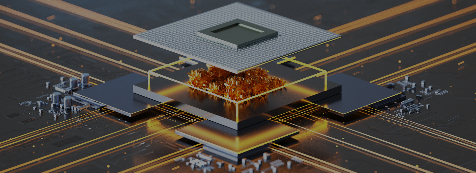
With the continuous evolution of AI computing power, optoelectronic chips, as the core components of optical communication, are facing huge market demand and technical challenges. The advent of the era of large computing power has promoted the evolution and upgrading of optical communication technology, making high speed, integration, and large capacity the core demands of optical chips.

The
Challenge
There are many packaging processes of optical modules, which are different from the common semiconductor chip packaging, especially in the link of patch, wiring, lens coupling, there are certain technical barriers, and the quality of the process directly affects the yield or performance of the product. In the patch process, optoelectronics face some very specific challenges.
-
 Consider the key requirements of the actual production process and alignment
 -
 High precision pick and fit requirements
 -
 Multiple chip bonding technologies (epoxy, eutectic, dipping)
 -
 Patch efficiency needs to be cost-effective
 -
 Modular design, can meet the diversified functional needs of customers

Our Recommendation
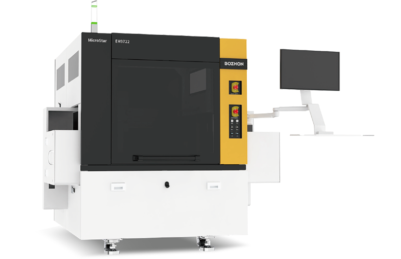
Optical module manufacturers need to adopt a variety of assembly techniques to solve the problem of alignment and fitting. Although active alignment of the launcher is an option, it is time-consuming and costly. As a result, processes utilizing high-precision and repeatable assembly platforms are more desirable, increasing production efficiency and reducing costs. This helps ensure accurate alignment during optical fitting, while accommodating a variety of mounting technologies to meet manufacturers' needs.Therefore, considering the solutions needed to meet these challenges, we recommend the MicroStar series EH9722 fully automatic high-precision eutectic die bonding machine.
Discover how we
can help you?


